Rational design and construction of [Si/SiO2]N one-dimensional photonic crystal for low infrared emissivity and visible light camouflage
一、 Research Background:
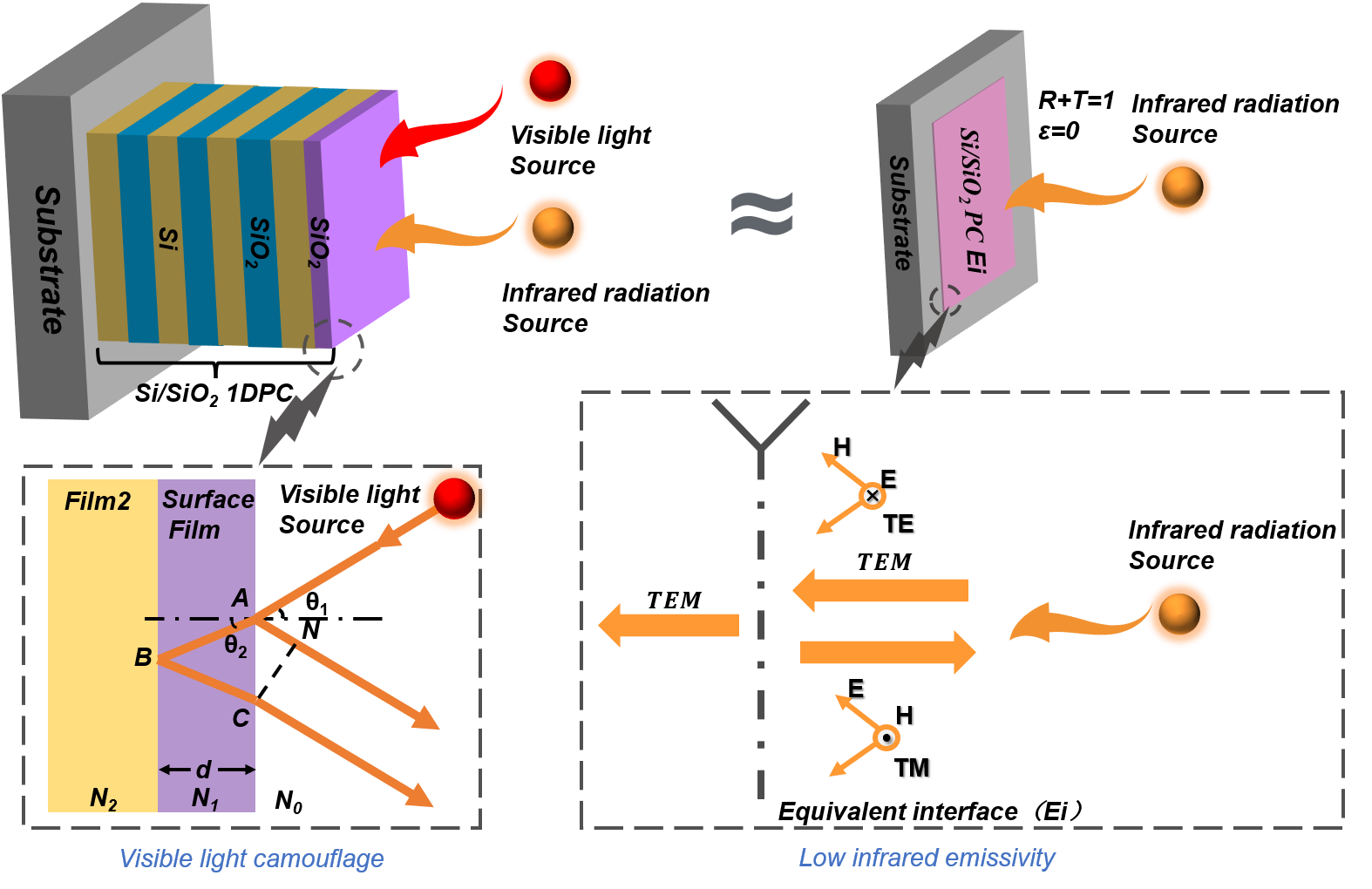
With the widespread use of infrared imaging detectors, low infrared emissivity has become an important direction in the development of military technology. According to Kirchhoff infrared theory, the emissivity of an object is proportional to its absorbance. Therefore, it is necessary to find materials with high reflectivity and low absorbance properties to achieve low IR emissivity at atmospheric window wavelengths. Conventional materials usually use metals or semiconductors as substrates, which cannot obtain low emissivity (ε<0.2) as well as selective low emissivity effects, making it more difficult to achieve compatible stealth. Therefore, metamaterials and new structures have received great attention. As a typical metamaterial, photonic crystals with photonic band gaps have been widely used in sensors, filters, solar cells, fabrics, and other fields. The material composition and dimensions of photonic crystals can be reasonably designed so that the photonic band gap covers the atmospheric window band and meets the requirements of low infrared emissivity. The effect of selective low emissivity and multi-band stealth can be obtained by adjusting the uneven distribution of the thickness of each sub-layer or stacking photonic crystals with different central wavelengths. Meanwhile, photonic crystals can affect isotropic interference by changing the thickness of the surface layer to show different colors, which is used to reduce the color contrast with the surrounding environment and achieve the effect that cannot be detected with visible light.
二、 Article Introduction:
In response to the above problems, the Laboratory has chosen Si materials with abundant reserves and mature purification technology. Si and its oxide SiO2 have stable chemical properties, high hardness, low coefficient of thermal expansion and good moisture resistance under service conditions. Si and SiO2 sub-layers can be obtained by direct or reactive sputtering of Si targets, which can be prepared in situ and integrated. First, the relationship between the process parameters and the optical properties of the sublayer is fully explored, and a preparation process with stable optical properties and high film-forming quality is determined. Then, a generic photonic crystal model is constructed based on the transmission matrix theory and the equivalent interface method, and the influencing factors of band gap width, position and reflectivity values are systematically simulated. Considering the complex working environment, the effects of incident angle, dispersion, extinction, film defects and other factors on reflectivity spectra were analyzed. Combining the results of the above simulations and calculations, the structure and preparation process of [Si/SiO2]N photonic crystals were optimized. Finally, [Si/SiO2]N photonic crystals with good low infrared emissivity and visible light artifact properties were successfully prepared. The related research results were published in optics and lasers in engineering. Yan-Ling Liu, a master's student, and Hongsheng Li, a doctoral student from Dalian University of Technology, are the first authors of the article, and Associate Professor Aimin Wu is the corresponding author.

Fig. 1 The illustration of the [Si/SiO2]N photonic crystal (PC) for visible light camouflage and low infrared emissivity.
三、 Research Content:
1. Using magnetron sputtering method to prepare Si and SiO2 monolayer films under different parameters, to investigate the relationship between sputtering power, substrate temperature, working air pressure, deposition time, magnetic field strength and oxygen partial pressure with optical properties and deposition rate, and to obtain a film preparation process with excellent optical properties, high deposition rate and good quality of film formation.
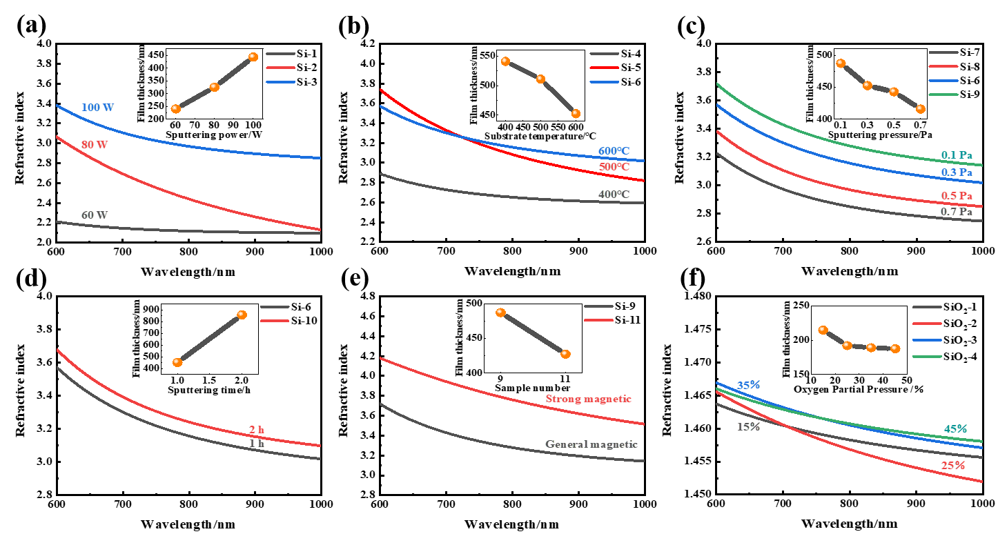
Fig. 2 The effect of different conditions for refractive index and sublayer thickness.
2、According to the transmission matrix theory for single interface, single-layer film and multi-layer film, we construct a general photonic crystal model under all-factor conditions and simulate the relationship between the forbidden band width, forbidden band center position and reflectivity value of photonic crystal and the influencing factors (refractive index ratio, period, central wavelength and optical thickness ratio). The effects of external factors (incident angle), structural factors (period, structure design, size) and material factors (dispersion, extinction, film defects) on the infrared reflectance spectrum are further investigated in the context of the actual working environment. The structure and preparation process of [Si/SiO2]N photonic crystals are optimized by taking into account the simulation results and the "thinning" effect.
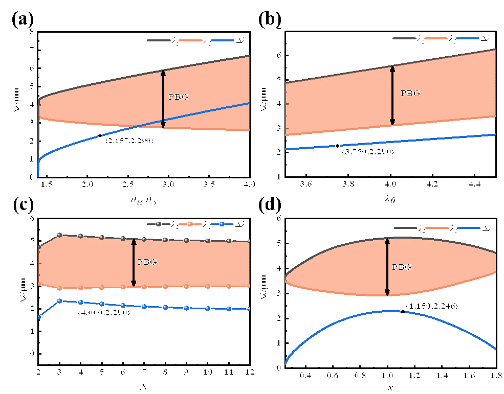
Fig. 3 The effect of different [Si/SiO2]N photonic crystal parameters for photonic band gap (PBG).
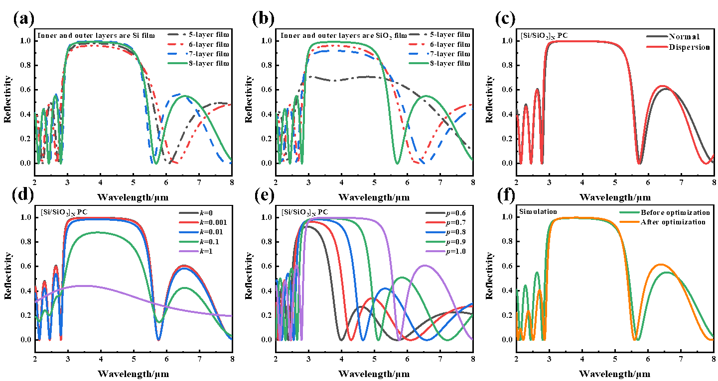
Fig. 4. Simulated reflection spectra of [Si/SiO2]N photonic crystals (PC) for different factors.
3. The average reflectance of the [Si/SiO2]N photonic crystal prepared under the guidance of simulation results is 95.23% in the 3~5 μm band, and the band range of the high reflection region is 2.914~4.868 μm, which covers most of the target band and shows excellent low infrared emission performance. By controlling the thickness of the photonic crystal surface layer, different colors of photonic crystals, such as orange, sandy yellow, dark green, navy blue and purple, were successfully prepared, which can meet the requirements of visible light camouflage in different environments.
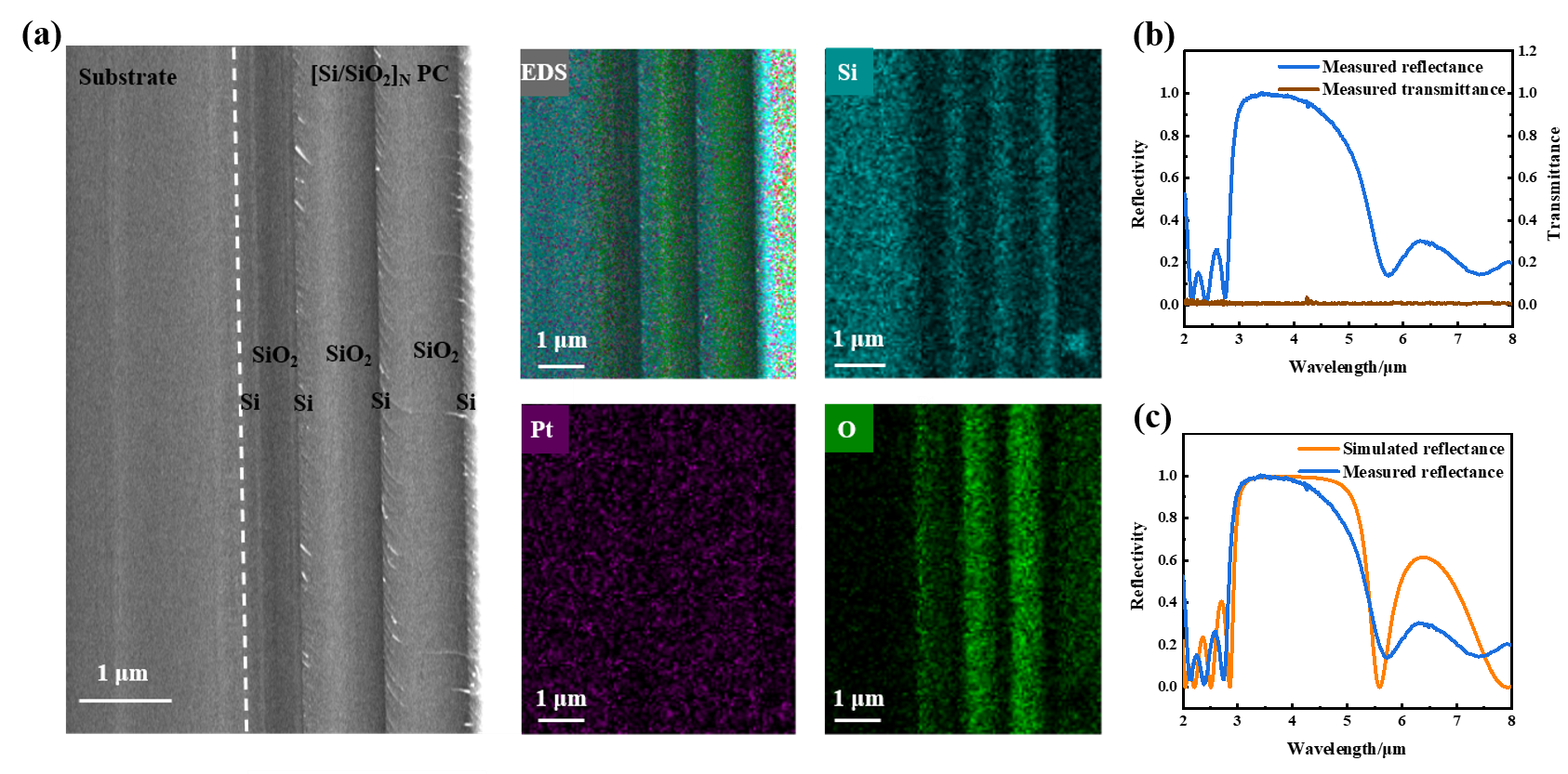
Fig. 5. SEM image and reflectance spectrum of [Si/SiO2]N photonic crystal cross section.
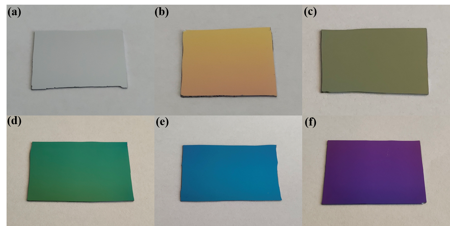
Fig. 6. Structural colors of [Si/SiO2]N photonic crystals with different surface layer thicknesses.
四、 Conclusion and Outlook:
In this paper, we successfully constructed a generalized photonic crystal model under all-factor conditions and simulated that the low infrared emissivity and visible light artifact properties of [Si/SiO2]N photonic crystals remain stable under the conditions of incidence angle, dispersion, extinction and film defects. The photonic band gap of the prepared [Si/SiO2]N photonic crystals covered the atmospheric window band of 3~5 μm, and the average reflectivity reached 95.23%. By adjusting the surface thickness of SiO2, five structural colors of orange, sandy yellow, dark green, dark blue and purple can be obtained. This synthetic strategy with environmental adaptability, reasonable process optimization, and suitable for mass production is expected to be widely used in military targets to cope with the increasingly complex warfare environment.
五、 Acknowledgements:
We thank the National Key Research and Development Program of China (2019YFA0709100 and 2020YFA0714504) and the Liaoning Province Revitalization Talent Program (XLYC1807237) for their support.
Authors:Yanling Liu, Hongsheng Li, Hanxiang Tong, Aimin Wu, Hao Huang, Tun Cao, Ang Ding
Title:Rational design and construction of [Si/SiO2]N one-dimensional photonic crystal for low infrared emissivity and visible light camouflage
Published in:Optics and Lasers in Engineering, doi: 10.1016/j.optlaseng.2023.107641

